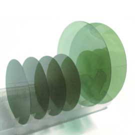
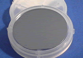
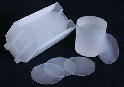
1.Si Wafer
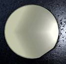
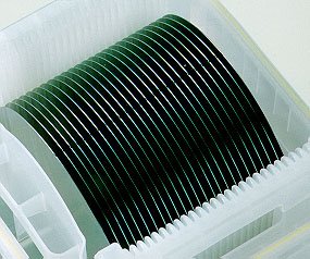
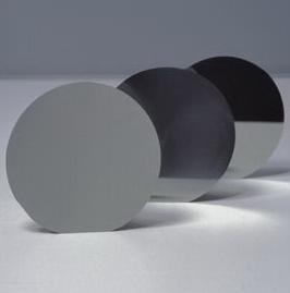
2”~12”, Single Side Polished & Double Side Polished, P-Type & N-Type, Resistivity: Low ( 1000 ohm-cm, FZ Process), Circular & Rectangular, Grade : Prime / Test / Dummy, Direction : , ,
2. Special Si Wafer :
With Thermal Oxides, SOI (Silicon On Insulation)
3. Glass Substrate :
Corning E2000 & XG Glass (25~300mm, 0.5~1.1mm Thick), Schott D263T, Pyrex,Other Optical Glass (BK7, …)
4. ITO Coated Glass :
< 15 ohm/cm2, Transmittance > 85%, 1200A, 400x370x0.7mm
5. GaAs :
2”~4”, Semi-Conductiong / Semi-Insulating, N-Type & P-Type, EPD < 5000 (LED) & < 500 (LD)
6. Sapphire (Al2O3) :
2”~6”, C-Plane (for LED) & R-Plane (for HTS), Single Side Polished & Double Side Polished
7. Ge:
2”~4”, Semiconducting, N-Type, EPD < 500, 170~350um Thick
8. SiC :
2” & 3”, Conducting (0.1 ohm-cm) & Semi-Insulating (> 105 ohm-cm), 4H & 6H, C-Plane
9. ZnO :
10x10mm, 20x20mm, 1”, C-Plane, Undoped, (10-10) & (11-20), FWHM < 30”
10. LiNbO3 & LiTaO3 :
For SAW application, 2”~4”, X-Y-Z Cut
11. HTS Substrate :
LaAlO3, SrTiO3, MgO, Sapphire, MgO, LSAT, YSZ
12. Special Substrate :
GaP, InP, GaSb, InSb, InAs, Quartz (SiO2), AlN, NaCl, MgF2, CaF2, ...


